
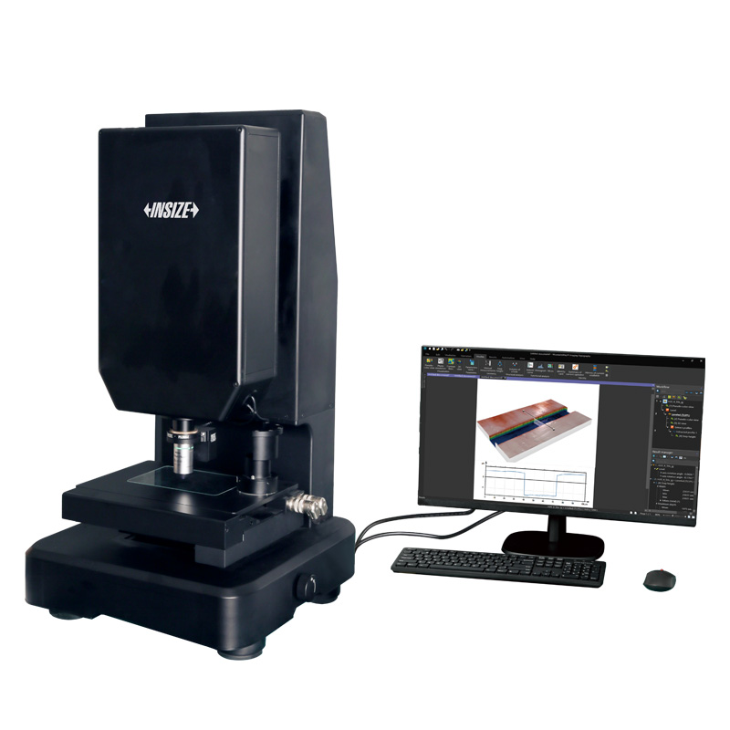
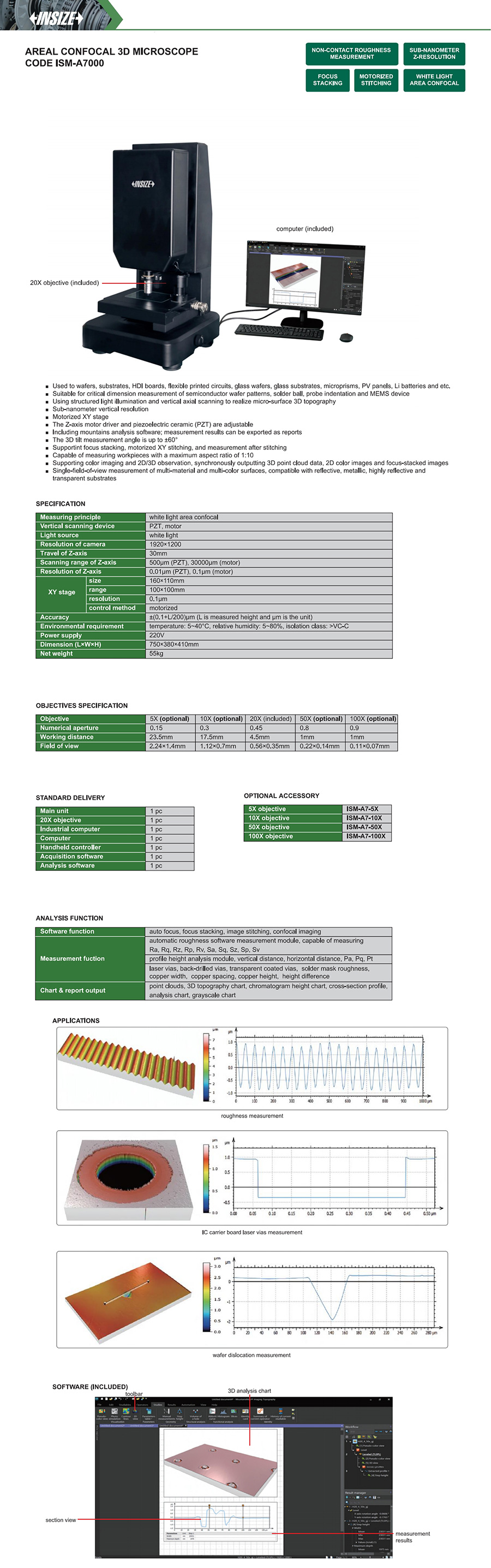
Areal Confocal 3D Microscope
Code: ISM-A7000
Used to wafers, substrates, HDI boards, flexible printed circuits, glass wafers, glass substrates, microprisms, PV panels, Li batteries and etc.
Suitable for critical dimension measurement of semiconductor wafer patterns, solder ball, probe indentation and MEMS device
Using structured light illumination and vertical axial scanning to realize micro-surface 3D topography
Sub-nanometer vertical resolution
Motorized XY stage
The Z-axis motor driver and piezoelectric ceramic (PZT) are adjustable
Including mountains analysis software; measurement results can be exported as reports
The 3D tilt measurement angle is up to ±60°
Supportint focus stacking, motorized XY stitching, and measurement after stitching
Capable of measuring workpieces with a maximum aspect ratio of 1:10
Supporting color imaging and 2D/3D observation, synchronously outputting 3D point cloud data, 2D color images and focus-stacked images
Single-field-of-view measurement of multi-material and multi-color surfaces, compatible with reflective, metallic, highly reflective and transparent substrates
| Code | Type | Magnification | View field | Pixel |
|---|---|---|---|---|
| ISM-A7000 | white light interference measuring microscope | 15-100X | 0.29*0.16~2*1.2mm | 2M |


View the complete
product specifications